
Illustrative engineering study · September 28, 2026
Sensor Enclosure: PCB Positioning and Connector Alignment
Follow the connector back to the features that locate its board before changing the opening in the housing.
The design question
What makes the connector line up with the window?
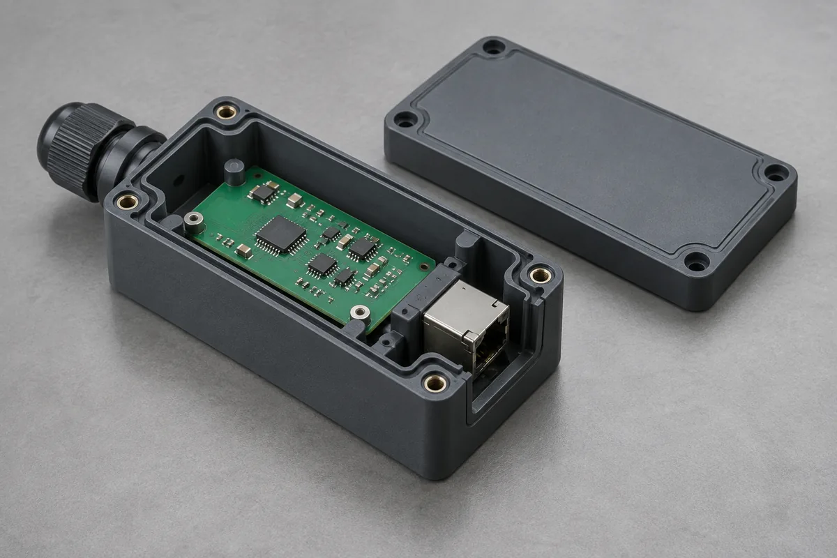
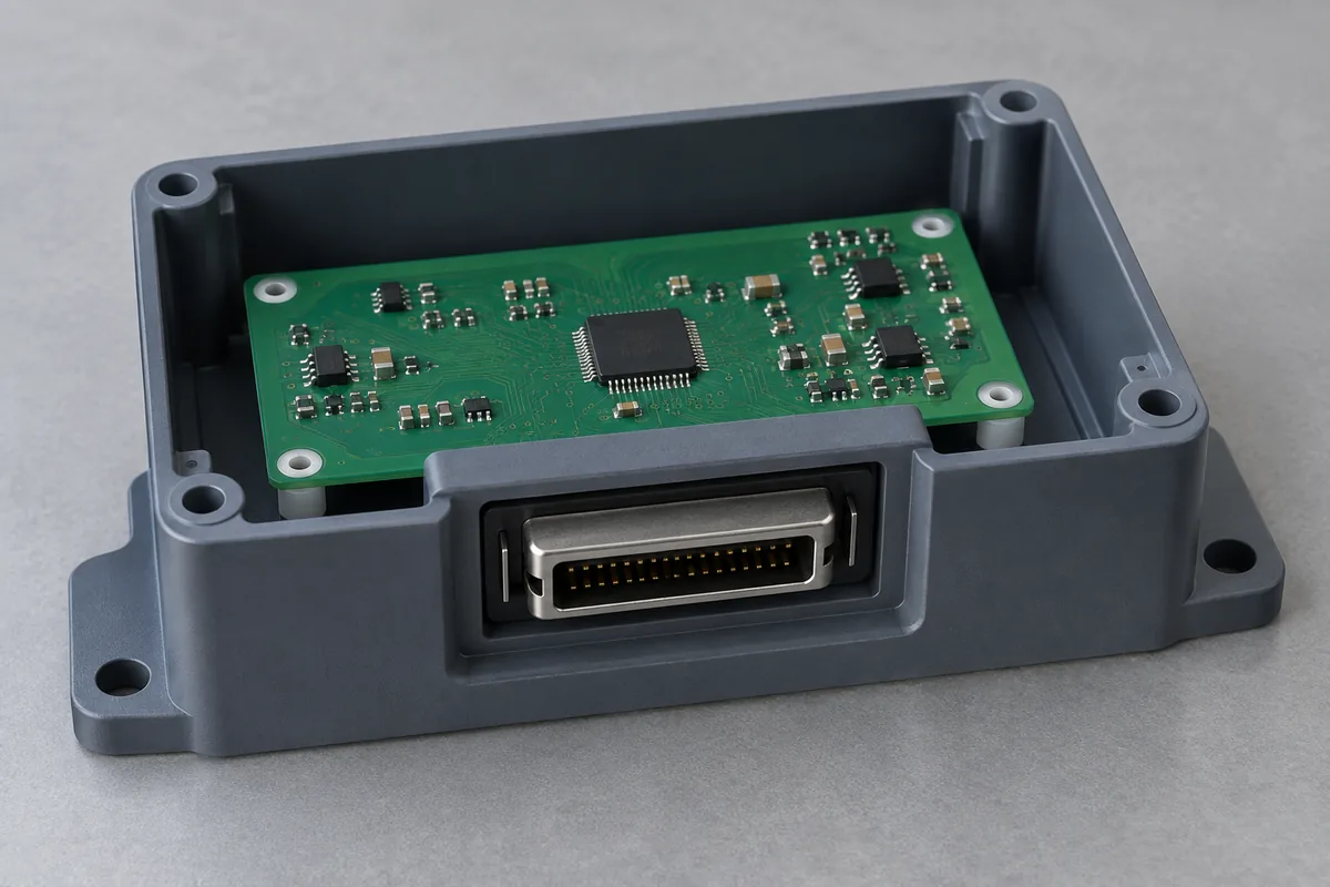
Consider a compact sensor with a rectangular PCB inside a two-piece molded enclosure. A board-edge connector must remain accessible through an end-wall opening. The base provides board supports, while separate fasteners retain the board and close the lid. Material grade, dimensions, tolerances and test requirements have not been approved in this example.
The review asks how the connector's position is established. If the board is fastened through clearance holes, its final sideways position may depend on the assembly freedom and tightening sequence. If additional locators are introduced, their fit and spacing must agree with the board. Simply adding a closer-fitting hole can exchange visible misalignment for difficult assembly.
Keep the board outline, connector definition and intended cable access common while comparing the locating concepts. Otherwise an enlarged window or moved connector can obscure what the proposed housing feature actually changes. Any alteration to the counterpart belongs in the decision record.
Two locating concepts
Fastener clearance or deliberately defined location?
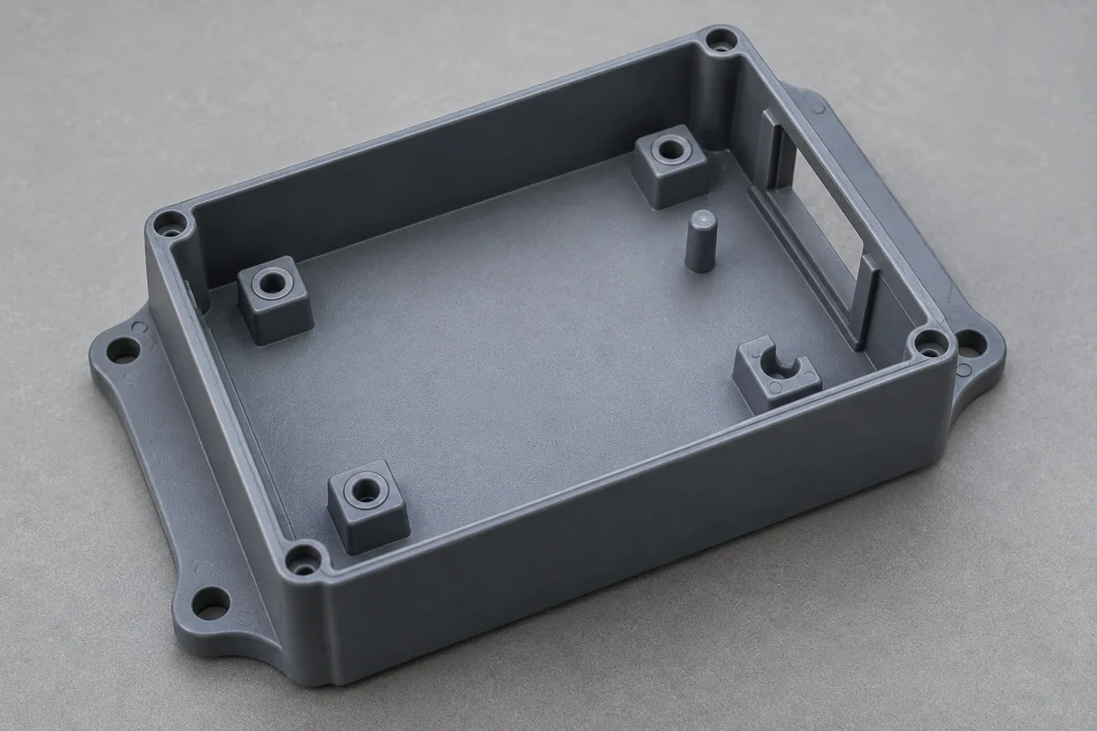
Concept A retains the PCB with screws through clearance holes and relies on the available assembly freedom. Concept B uses a defined support plane with a primary locator and a relieved secondary locating relationship, while retaining screws perform their specified fastening role. The concepts are discussion options, not approved designs.
For A, ask whether the full range of permitted board positions still leaves sufficient connector clearance and cable access. A floating arrangement can be acceptable when the interface accommodates it deliberately. It should not be described as repeatable precision location without evidence.
For B, ask which motions each feature constrains, whether the PCB can seat without force, and whether the locators can be molded and inspected reliably. Consider hole-to-hole variation and thermal effects using the actual materials and requirements. A relieved locator must be defined by an engineer; the phrase alone does not specify a fit.
The two paths in the diagram share a housing reference. One leads through the board location to the connector. The other leads to the opening. Their relationship, together with local geometry and the mating plug, determines the relevant clearance question. No tolerance or statistical yield is inferred from the drawing.
Interface review
Separate lateral alignment from vertical seating.
A board that is correctly located sideways can still place the connector at the wrong height. Review support-pad height, board thickness, component mounting and the connector envelope. Check that the board is actually seated on the intended supports rather than on an unintended rib or trapped component.
Review the mating plug as well as the receptacle. The cable overmold or insertion angle can require access beyond the connector's visible metal shell. Distinguish free clearance around the shell from any intentional contact or sealing feature. This study assumes no environmental rating and does not design a connector seal.
| Interface | Inputs to resolve | Proposed evidence |
|---|---|---|
| Board support | Support features, board contact zones and permitted restraint. | Feature measurements and an observed seating check in the agreed state. |
| Board location | PCB hole definitions, locators and the intended freedom. | Datum-based measurements and an assembly check without undocumented forcing. |
| Connector window | Connector envelope, placement requirements, opening form and mating plug. | Clearance analysis plus the agreed physical access check. |
| Lid and fastening | Internal height, screw engagement, sequence and closure requirements. | Empty-housing comparison followed by populated-assembly evaluation. |
Use exact-grade information if material candidates are compared. Covestro's housing-material overview shows that different resin formulations serve different housing requirements; it does not qualify this hypothetical sensor. A resin choice must remain connected to geometry, processing and the actual environment.
Proposed verification
Add constraints in a documented sequence.
First inspect identified empty housing samples under the agreed support condition. Then check the empty lid-to-base fit. Next install the controlled PCB and connector configuration, observing seating and location before retention is finalized. Finally close the cover using the specified method and evaluate the required access and seam characteristics.
This sequence helps distinguish a housing-form issue from board location, component height or fastening. It does not require a universal sample count. Sampling should be agreed for the development stage, tool cavities and decisions being made, with part identity preserved through the sequence.
Record material, drawing revision, cavity, molding run, PCB revision, connector identity and inspection setup as appropriate. A development board with hand-enlarged mounting holes is a modified specimen; it must not silently become the acceptance counterpart. Similarly, a relieved housing window represents a changed configuration.
If a trial exposes a problem, retain the original observations and change one documented configuration at a time where practical. Pair component measurements with assembly observations. A successful cable insertion is useful evidence of that particular check, not proof of every drawing characteristic or long-term connector reliability.
Decision boundary
The deliverable is a review plan, not an invented success metric.
A real review might retain controlled board float, develop dedicated locators, adjust the window or revise the assembly reference. The choice depends on the actual drawings and evidence. Neither concept in this study has demonstrated lower scrap, tighter positioning or faster assembly.
Before tooling release, assign responsibility for the PCB and connector definitions, locating scheme, critical dimensions, fixture design and finished-device qualification. Close unresolved assumptions in writing. After trials, compare identified results with the agreed criteria and record any authorized deviations.
The useful output is a traceable path from an interface requirement to a drawing, a molding proposal and an inspection decision. It gives the buyer a clearer quotation scope while keeping unsupported claims out of the approval record. For the broader starting checklist, see our plastic enclosure design guide.
Apply the review to your part
Turn your drawing into a defined review.
Send the base, lid, populated-board envelope and mating-connector information with the intended use and unresolved fit questions. Keep a proposed design change distinguishable from a tested result.
Explore our custom injection-molded electronic enclosures or the broader injection molding service.