
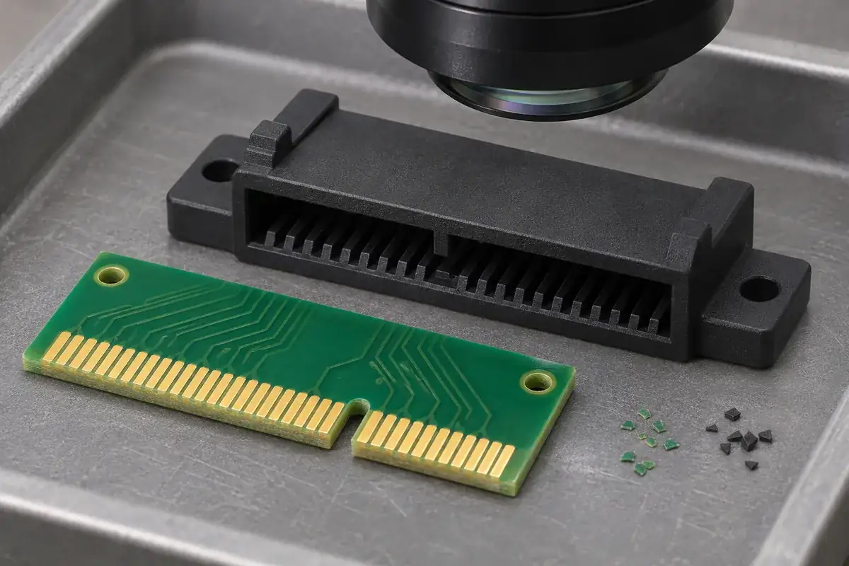
A few particles found after a card is inserted can lead quickly to a request for a wider connector slot. That may be the right change, but the particles could also originate at a rough board edge, a damaged key, contamination left from another operation or the contact interface. The location and material of the debris need to be investigated before a dimensional correction is selected.
Start by preserving the condition in which the observation occurred. Identify the board and connector revisions, note whether either part was previously used, and record the insertion sequence. Cleaning everything and repeating the assembly many times can erase the original evidence while adding new damage that makes the cause harder to isolate.
Product design illustrations accompany the interface and manufacturing explanations below.
Distinguish particle appearance from material identification
Color can suggest a source but does not establish it. A dark particle is not automatically housing resin, and a bright particle is not necessarily contact plating. Lighting, contamination and mixed material can make visual interpretation unreliable. Use suitable magnification and, where the investigation requires it, an appropriate material-identification method.
Record where particles are found before moving the assembly. Material at the slot entrance can point to a different stage from material deeper in the contact region. The collection location is still not proof of origin because particles can move during insertion, removal or handling. Treat it as one clue to compare with surface marks and the assembly path.
Compare unused parts with the parts involved in the observation. Incoming debris on an untouched board or housing changes the investigation from wear generation to cleanliness or handling. Keep that distinction visible in the record so a cleaning problem is not automatically converted into a tooling change or a complaint about the contact design.
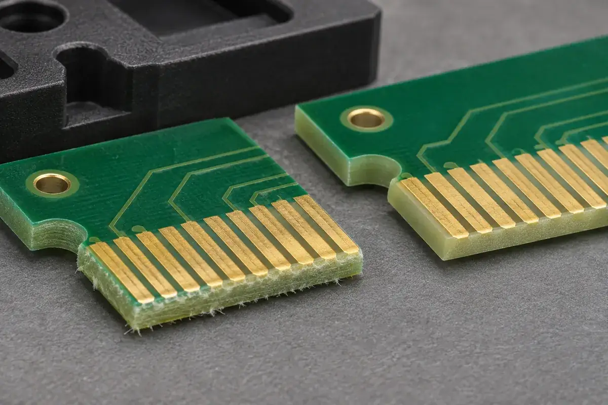
The board's leading edge deserves a close look. Local roughness, an incomplete bevel or a damaged corner can produce a repeatable catch. The relevant feature may be small compared with the overall board thickness. Inspect the location where the board first meets the housing and compare it with the corresponding mark on the plastic.
Look for a localized plastic contact path
A continuous rub along one wall suggests a different relationship from a single damaged corner. Compare the witness location with the board's outline, thickness and approach angle. A board may be within its nominal thickness range yet touch one side because a guide or mounting feature directs it away from the intended center plane.
Inspect the slot entrance for flash, burrs or an inward step between molded features. Small local obstructions can be missed when only overall slot width is measured. If the part comes from multiple cavities, retain that identity during the review. The investigation should distinguish a systematic design conflict from a local tooling or process condition.
A polarizing key is another possible contact location. A notch can clear the key near the mouth but catch at a shoulder farther into the socket. Review the complete profiles and the travel path. Simply widening the notch at its opening may leave the deeper interference untouched and weaken the intended orientation control.
Where the construction allows it, an empty-housing comparison can help isolate plastic interference from the metal contact system. Keep the board and fixture conditions equivalent. The comparison answers a limited question about the source of resistance; it does not qualify the completed connector or establish that a housing modification is acceptable without further review.
Evaluate the contact region using its own requirements
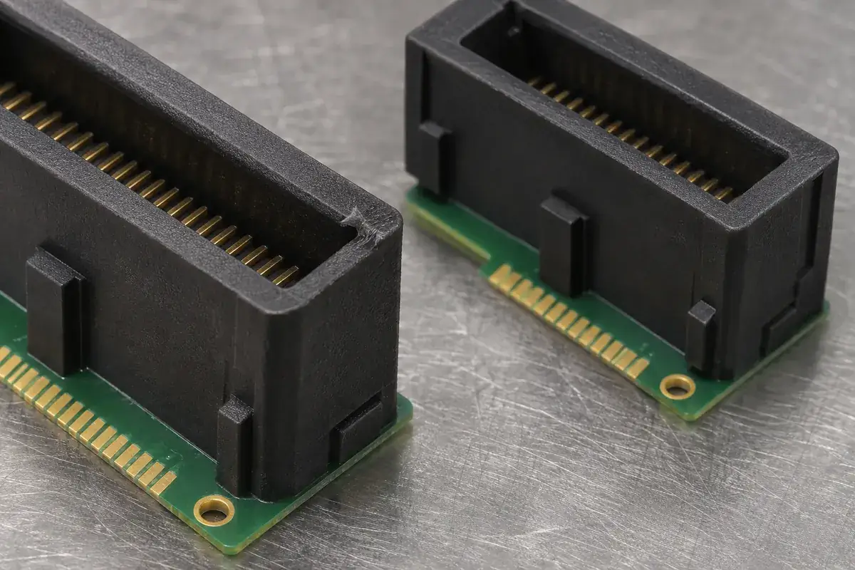
Contact surfaces are designed to interact during mating, so an observed mark is not automatically a failure. At the same time, visible scraping or material transfer should not be dismissed as normal without reference to the connector's acceptance criteria. Separate expected contact interaction from damage caused by an unsuitable board finish, misalignment or unintended travel.
Samtec's connector-plating discussion explains that surface finish affects wear and other contact behavior. The relevant finish is therefore part of the mating-system definition, not a cosmetic board choice. Evaluate the specified board and contact finishes together rather than attributing every particle to plastic clearance.
Review where the contact works on the pad at the final installed position. A contact that reaches an unintended edge or transition may behave differently from the approved arrangement. The related contact-wipe and insertion-stop guide explains why total board travel is not a substitute for that relationship.
Do not continue cycling a visibly damaged sample simply to obtain more observations. Additional insertions can alter the contact, spread particles and create new witness marks. Agree an investigation sequence that preserves useful evidence. If cycling is part of a defined test, keep that test and its acceptance criteria separate from an informal troubleshooting trial.
Make a correction that addresses the identified cause
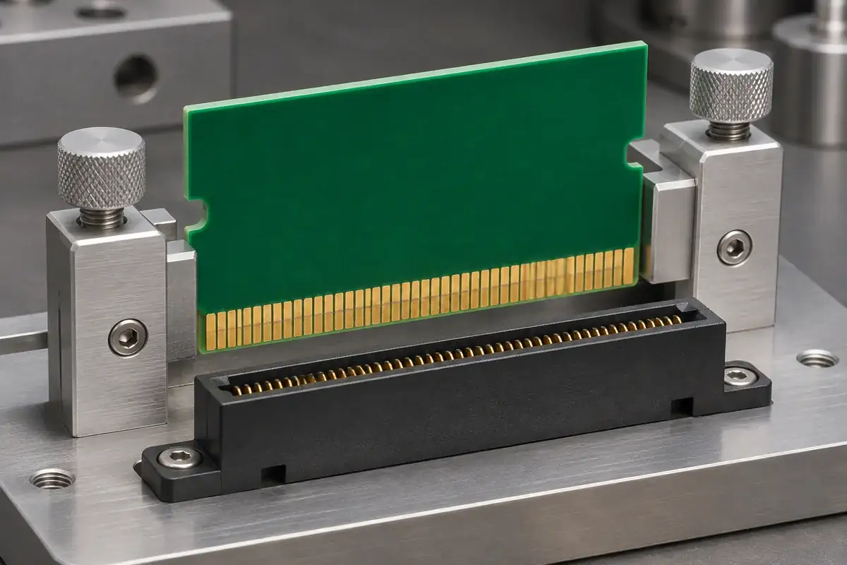
A board-edge correction, a housing-tool correction and an assembly-guide correction solve different problems. Select the change after the evidence identifies the interfering features. Document which variable changed and compare the resulting condition using the same controlled references. Otherwise several simultaneous changes can make a successful sample difficult to reproduce.
If the board edge is involved, coordinate the bevel and housing entrance rather than removing material by hand without a drawing update. If the approach is involved, review the guide position and insertion method. Each correction should become part of the controlled interface or process definition.
After a proposed correction, evaluate more than the absence of visible particles in one trial. Confirm the relevant fit and contact requirements, the sample condition and any specified cleanliness criteria. A cleaner-looking assembly is useful evidence, but it does not automatically demonstrate electrical performance or durability under the application's required conditions.
For custom molded card-edge housings, send photographs of the observed locations together with board and housing drawings, sample history and the assembly sequence. Clear evidence lets the review focus on the actual interference and the inspection method needed to verify its correction, rather than starting with an unsupported request to enlarge the slot.