
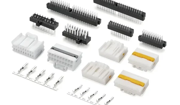
| Electrical connectors are manufactured in four sequential stages: (1) Stamping, where high-speed progressive dies form metal contacts from copper alloy strip at 200–800 strokes per minute; (2) Electroplating, where contact surfaces receive gold, palladium-nickel, silver, or tin coatings; (3) Injection molding, which forms the insulating polymer housing; (4) Assembly, where plated contacts are inserted into the housing and the complete connector is tested to applicable performance standards. |
These four stages are performed in sequence because each depends on the output of the previous: the stamped contact geometry must be established before plating can be applied to contact surfaces; the housing geometry must accommodate the plated contact dimensions; and assembly requires both to be complete and inspected before mating.
This guide covers each stage in depth — process parameters, materials used at each stage, inspection methods applied, and the standards that govern final product qualification.
Connector Anatomy: What an Electrical Connector Contains
Every electrical connector, from a micro USB connector to a large circular military connector, consists of the same three functional element groups. Understanding these groups clarifies why each manufacturing stage exists. You’ll typically find a few key players:
Housing
The housing is the insulating outer shell that positions contacts at the correct pitch and depth, protects the contact assembly from mechanical damage, and provides the mechanical interface — latches, threads, bayonet lugs — that holds mated connectors together under vibration and thermal cycling.
Housings are almost always injection-moulded polymer for commercial applications. Metal housings (die-cast aluminium or zinc) are used where electromagnetic shielding or structural ruggedness requirements exceed what polymer can provide.
Contacts
Contacts are the conductive elements that carry current or signal across the mating interface. They maintain a defined contact force — typically 50–300 g normal force — through the rated mating cycle life. Contact force determines contact area, which in turn determines contact resistance and heat generation under load.
The physics relationship: contact resistance R = ρ × l / A, where resistivity ρ is set by the plating material, and contact area A decreases as contact force decreases over mating cycles. A connector specified for 10 A that develops 50 mΩ contact resistance from worn contacts dissipates 5 W at the contact interface — sufficient to cause thermal damage in compact assemblies.
Terminals and Inserts
Terminals provide the wire-to-contact interface — crimp barrels, solder cups, or IDC (insulation displacement contact) features that join the external conductor to the connector’s internal contact system. Inserts or wafers — molded polymer or elastomer components — position individual contacts relative to each other within the housing, maintaining creepage and clearance distances required by IEC 60664-1 at the working voltage.
Common Connector Types
There’s a whole universe of different types of electrical connectors out there, each designed for specific jobs. You’ve got:
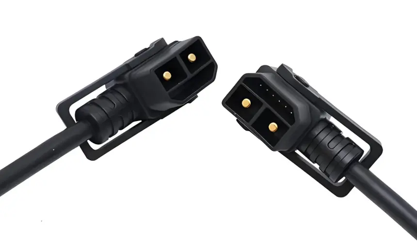
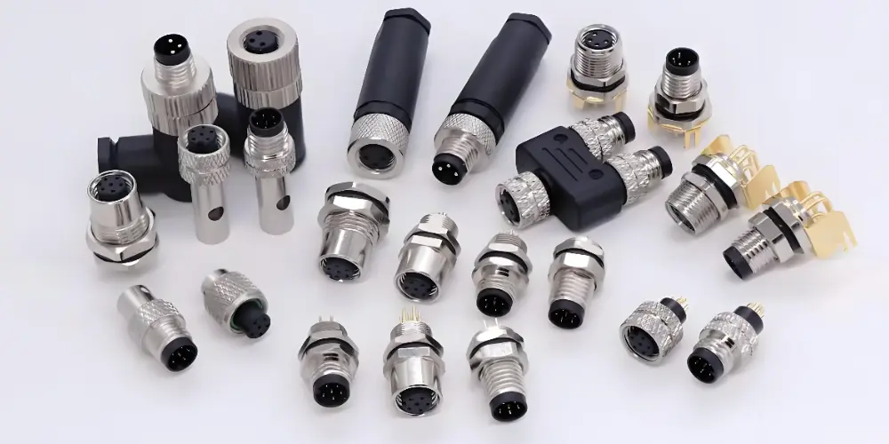
- Circular connectors: MIL-DTL-38999, M12, M8 — rugged, easy to seal, common in aerospace, military, and industrial automation.
- PCB connectors: Board-to-board, wire-to-board — the highest unit-volume connector category. Sub-millimeter pitch board-to-board connectors drive demand for LCP housings and precision progressive die stamping.
- RF connectors: SMA, N-type, SMP — 50 Ω or 75 Ω impedance-controlled for microwave frequency signals. Center contact geometry determines impedance; housing and backshell design determines shielding effectiveness.
- Fiber optic connectors: LC, SC, MTP — transmit information via light rather than electrical signal. Ceramic or zirconia ferrule alignment to within 0.5 µm is the precision manufacturing challenge.
Materials for Connector Manufacturing
Material selection drives both performance and manufacturing feasibility. Housing material determines operating temperature range and the minimum wall section achievable in injection molding. Contact base metal determines spring stiffness, conductivity, and cycle-life capability. Plating material determines contact resistance stability over the connector’s service life.
Housing Materials
| Material | Class | Key Properties | Connector Application Notes |
| PBT (Polybutylene terephthalate) | Thermoplastic | HDT 200–210°C; UL 94 V-0; low moisture absorption < 0.08%; excellent dimensional stability | Most common connector housing resin. Automotive, industrial controls, consumer electronics. Balance of cost, processability, and thermal performance. |
| LCP (Liquid Crystal Polymer) | Thermoplastic | Shrinkage < 0.1%; wall sections to 0.2 mm; HDT > 250°C; UL 94 V-0 | Micro-pitch connectors (0.3–0.5 mm pitch) in smartphones, hearing aids, wearable devices. Rapid solidification requires gates within 150 mm of the furthest feature. |
| PPS (Polyphenylene sulfide) | Thermoplastic | Continuous service to 220°C; excellent chemical resistance; UL 94 V-0 | High-temperature underhood automotive connectors, aerospace sensor housings, industrial chemical environments. |
| PA66 / PA46 (Polyamide / Nylon) | Thermoplastic | Good impact toughness; moisture absorption 2.5–3.5% — pre-dry required; wide material availability | Lower-cost industrial and consumer connectors where moisture dimensional change is tolerable. GF-reinforced grades used for stiff precision housings. |
| Aluminium (A380 die-cast or 6061 machined) | Metal | High strength; thermal conductivity 96–167 W/(m·K); excellent EMI shielding > 60 dB | Military (MIL-DTL-38999), aerospace rack-and-panel, industrial DIN housings where shielding or environmental sealing is critical. |
Contact Base Materials
| Material | Class | Key Properties | Application |
| Phosphor bronze (Cu-Sn-P alloy) | Copper alloy | Spring stiffness with fatigue resistance; conductivity ~15% IACS; easily stamped | Contact arms and spring fingers where repeated deflection is required. Standard for PCB edge connectors and card sockets. |
| Brass (C26000 / Cu-Zn) | Copper alloy | Conductivity ~28% IACS; good machinability; lower spring force than phosphor bronze | Pin contacts and crimp terminals. Widely used where dimensional accuracy and conductivity matter more than spring stiffness. |
| Beryllium copper (BeCu, C17200) | Copper alloy | Highest spring strength among copper alloys (HV 220–250); used for high-cycle-life contacts (> 10,000 matings) | High-reliability signal connectors, mil-spec applications. Requires special machining handling due to Be particle hazard. |
Connector Contact Plating — Performance Data
Plating is not merely protective decoration — it is the primary determinant of contact resistance, mating cycle life, and long-term reliability. The base copper alloy oxidizes rapidly in ambient air; the plating system is what maintains the low-resistance contact interface across the connector’s rated service life.
| Plating | Thickness | Performance Data | Application Context |
| Gold (Au) | 0.1–1.25 µm | Contact resistance < 10 mΩ; zero oxidation; 30+ year shelf life; MIL-DTL-55302 specifies 0.5–1.25 µm | Signal-level connectors (< 1 A); precision instruments; military/aerospace contacts. Selective plating on contact area only reduces Au consumption 40–70%. |
| Palladium-Nickel (PdNi, 80/20) | 0.1–0.5 µm | Harder than gold (HV 450–500 vs Au HV 100); fretting resistance; lower cost than gold | Telecom connectors (SFP, QSFP, SIM); high-cycle-life applications. Best balance of cost and durability for signal connectors. |
| Silver (Ag) | 2–10 µm | Highest bulk conductivity (6.3×10⁷ S/m); excellent for high-current contacts; tarnishes in sulfur environments | High-power connectors (> 100 A); EV battery pack terminals; bus bar contacts. Apply sulfur-resistant overcoat if exposed to industrial atmospheres. |
| Tin (Sn) | 1–5 µm | Solderable; contact resistance < 5 mΩ initially; tarnishes under repeated mating; prone to fretting corrosion | Low-cost PCB edge connectors; consumer electronics. Not recommended for high-cycle or vibration-critical applications — tin fretting produces resistive debris. |
| Nickel (Ni) underlayer | 1–3 µm (base layer) | Diffusion barrier between copper substrate and final finish; prevents Cu migration through Au under thermal cycling | Mandatory underlayer beneath gold or PdNi on all copper-alloy contacts. Without Ni, Cu migrates to gold surface within weeks at 125°C, forming resistive Cu oxide. |
The Four-Stage Electrical Connector Manufacturing Process
The four stages below follow a fixed sequence in production. The output quality from each stage gates the next — a dimensional defect in stamping propagates into plating yield, housing fit, and ultimately connector electrical performance. Quality inspection is embedded in each stage, not applied only at the end.
| # | Stage | Process Detail | Quality Verification |
| 1 | Stamping | Progressive die pressing of metal strip (Cu alloy, 0.1–0.8 mm thick) at 200–800 strokes/min; contacts formed to ±0.01–0.03 mm | Vision system inspects width, depth, spring arm geometry, contact face dimensions at > 600 parts/min; 100% of production |
| 2 | Electroplating | Reel-to-reel (strip still on carrier) or barrel (separated contacts) plating: alkaline clean → strike Ni → barrier Ni → selective Au/PdNi/Sn on contact areas | XRF thickness measurement per batch; cross-section analysis for pinholes; adhesion pull test per ASTM B571 |
| 3 | Injection molding | Engineering thermoplastic (PBT 230–260°C, LCP 300–330°C, PPS 310–340°C) injected into precision mould; housing formed in 15–45 s cycle | Backlit transmitted-light inspection for internal voids, short shots, and clogged contact retaining sockets; CMM on first-article and sampling basis |
| 4 | Assembly | Plated contacts inserted into housing pockets — automated insertion for volume production (50+ connectors/sec), manual for complex or low-volume designs; overmoulding and potting as required | 100% vision inspection for contact presence and seating depth; mating force measurement per IEC 60512-13; electrical continuity and isolation resistance test per IEC 60512-2 |
| 5 | Final test and traceability | Electrical performance: contact resistance, insulation resistance, dielectric withstand voltage; mechanical: mating/unmating force, locking force; environmental per application standard (USCAR-2 thermal shock; IP67 seal per IEC 60529 | Full batch record: resin lot, plating bath parameters, press die ID, inspection results — retained for design life plus statutory period |
Cold runner waste in connector housing molding can add material consumption. Hot runner systems can eliminate this waste and improve part-to-part consistency by eliminating the pressure drop through the runner that cold runner systems experience shot-to-shot. For LCP housing programs running millions of parts annually, the hot runner investment typically pays back in material savings within the first production quarter.
Stage-by-Stage Detail
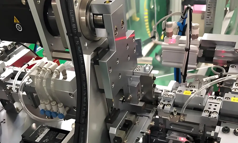
Lots are involved in turning basic material into a finished electrical connector, and there are several important manufacturing processes that are employed. Let’s take a look at the primary processes.
Stage 1: Stamping
Metal contacts and terminals are formed by progressive die stamping — the foundational process for all high-volume connector contact production. A metal strip (0.1–0.8 mm thick copper alloy) feeds from a coil through a multi-station progressive die at 200–800 strokes per minute.
Each station in the die performs a specific operation: piercing, blanking, bending, coining, or forming. By the time the strip exits the final station, fully formed contacts remain attached to the carrier strip — positioned for transfer to the plating line without individual handling, preserving the contact geometry against the damage that manual transfer would cause.
Progressive die tooling achieves contact dimensions to ±0.01–0.03 mm. Contact width, spring arm geometry, and the contact depression depth — all of which directly affect contact resistance and insertion force — are established in this stage and cannot be corrected downstream.
→ Related: Fecision metal stamping die design and manufacture
Stage 2: Electroplating
After stamping, the contact strip moves to the plating line. Reel-to-reel plating — where the contacts remain on the carrier strip throughout — preserves contact geometry and allows selective plating: applying gold only to the contact area and not the full contact body. Selective plating reduces gold consumption by 40–70% compared to full-body plating, while delivering identical contact performance.
Standard plating sequence for a gold-plated contact: electrolytic alkaline cleaning → strike nickel (thin adhesion layer) → barrier nickel (1–3 µm) → selective gold (0.1–1.25 µm per application specification). Each bath parameter — pH, temperature, current density — is monitored continuously. Deviation from specification triggers automatic line stop and batch isolation before non-conforming material advances to the molding stage.
Stage 3: Injection Molding of the Connector Housing
Engineering thermoplastics for connector housings require specific molding conditions that differ significantly from commodity resin practice. LCP at 300–330°C barrel temperature and injection velocities up to 500 mm/s fills wall sections as thin as 0.2 mm before the melt front freezes. PPS at 310–340°C requires pre-dried material (< 0.05% moisture) and controlled mold temperature (120–160°C) to achieve the crystallinity that delivers its heat and chemical resistance properties.
Multi-cavity connector housing tools (8-cavity to 64-cavity are common for high-volume PCB connector programs) demand precisely balanced runner systems — equal fill pressure and timing to every cavity. Cavity-to-cavity imbalance produces dimensional variation between housings from different cavities in the same shot, creating contact insertion force variation that causes assembly line stoppages.
→ Related: Fecision precision connector mold manufacturing
Stage 4: Assembly and Overmolding
Final assembly inserts plated contacts into housing pockets. For volume production, automated insertion machines handle contacts from vibratory feeders and press each into its housing pocket at defined depth and engagement force.
Overmolding — encapsulating a cable-contact assembly in a secondary polymer jacket — is performed as part of the assembly stage. It seals the wire-to-terminal junction against moisture and mechanical stress, provides strain relief, and can incorporate polarization keying into the completed assembly.
The overmold material must bond chemically or mechanically to the primary housing material — a materials compatibility requirement confirmed during DFM before tooling is cut.
Quality Control Across All Stages
Quality verification in connector manufacturing is not a single end-of-line inspection — it is a layered system applied within each stage. The key methods:
- Stamping inspection: High-speed vision cameras check contact shape, width, depth, and spring arm geometry at production speed (> 600 parts/min). Out-of-specification contacts trigger automatic rejection and press stop.
- Plating verification: XRF (X-ray fluorescence) thickness measurement checks gold, PdNi, and Ni deposit thickness against specification. Destructive cross-section analysis detects pinholes and adhesion failures at sampling frequency.
- Housing inspection: Backlit transmitted-light inspection identifies short shots, voids, and clogged contact retention sockets that external surface inspection cannot detect. CMM dimensional verification on first-article and statistically sampled production batches.
- Assembled connector testing: Contact resistance per IEC 60512-2; insulation resistance per IEC 60512-2; mating and unmating force per IEC 60512-13; IP sealing test per IEC 60529. USCAR-2 thermal shock (−40°C to 125°C, 500 cycles) for automotive connectors. [3]
- Traceability: Metal strip lot, plating bath parameters, resin lot, press die ID, operator (where applicable), and inspection results are recorded per batch and retained for design life plus statutory period per applicable quality standard.
Type-Specific Manufacturing Considerations
PCB Connectors: Precision at Scale
PCB (printed circuit board) connectors are the highest unit-volume connector category globally. Board-to-board connectors with 0.3–0.5 mm pitch require LCP housings (to achieve 0.2 mm wall sections and ±0.01 mm pin-pocket tolerances) and progressively stamped contacts with spring geometry accurate to ±0.02 mm to maintain consistent contact normal force across the full pin array.
At this pitch, pin coplanarity across a 50-way array must be within ±0.05 mm — deviations beyond this cause uneven mating force that prevents automatic SMT pick-and-place or causes missed connections at individual pins. CMM verification of coplanarity on first-article samples and periodic production sampling is the standard process for PCB connector tooling qualification.
Circular Connectors: Sealing and Environmental Performance
Circular connectors for industrial and military applications (MIL-DTL-38999, USCAR series, M12) incorporate elastomeric face seals, backshell overmolds, and rigid metal shells that must meet IP67 or IP68 sealing requirements per IEC 60529. The shell is typically die-cast aluminium or zinc, then CNC-machined on sealing surfaces and threaded features to ±0.05 mm.
Shell concentricity — the alignment between the contact insert bore and the external shell thread — is the critical dimension. Non-concentric shells prevent correct mating and compress the face seal unevenly, producing a leak path at the point of maximum misalignment. Shell concentricity is verified on CMM after final machining, with rejection criteria typically ±0.025 mm.
RF Connectors: Impedance Control Through Geometry
RF connector performance is determined by the characteristic impedance of the transition region — the geometry between the external cable shield and the connector’s internal signal path. For a 50 Ω SMA connector, the center contact diameter, the dielectric insert geometry, and the shell bore must all be held to tolerances that keep impedance within ±2 Ω across the design frequency range.
Dimensional deviations that would be cosmetically invisible at DC produce measurable reflections (return loss degradation) at GHz frequencies. RF connectors are verified by vector network analyzer (VNA) measurement of S-parameters — insertion loss and return loss — not just dimensional inspection.
Custom Connector Manufacturing at Fecision
Fecision’s connector manufacturing capability covers both the tooling and production stages of the process — progressive stamping die design and manufacture, precision connector mold tooling, and injection molded housing production.
- Stamping die design and manufacture: Progressive dies for contacts from 0.1 mm sheet to precision strip tolerances of ±0.01–0.02 mm. Multi-stage designs covering pierce, blank, form, and coin operations in a single die sequence.
- Connector mold tooling: CNC and EDM machining to ±0.003–0.005 mm on critical cavity features. LCP and PPS hot runner tools, multi-cavity balanced runners up to 64 cavities. DFM review before tooling commitment, Moldex3D simulation for fill and weld-line analysis.
- Housing injection molding: PBT, LCP, PPS, PA66, PC — all in current production. ISO 9001:2015 certified. CMM first-article inspection with Cpk ≥ 1.33 on critical dimensions.
- Documentation: DFM review report, mould flow simulation output, first-article CMM report, dimensional data, and material CoA provided with every completed tool and production order.
Contact Fecision for a DFM review and tooling quote at fecision.com/contact-us.
Frequently Asked Questions
Why is a nickel underlayer needed under gold plating?
Copper diffuses through gold at elevated temperatures, forming copper oxide at the surface and increasing contact resistance from < 10 mΩ to > 100 mΩ within weeks at 125°C. A 1–3 µm nickel barrier layer between the copper substrate and gold finish blocks this diffusion and maintains contact resistance stability throughout the connector’s service life.
What materials are used for connector housings and why?
PBT is the broadest-use connector housing resin — balanced cost, thermal performance (HDT 210°C), and dimensional stability. LCP is specified for micro-pitch connectors (0.3–0.5 mm pitch) where wall sections below 0.3 mm are required, because its shrinkage below 0.1% delivers the tightest tolerances. PPS is selected for high-temperature environments above 150°C continuous service.
What standards govern connector manufacturing quality?
- IPC/WHMA-A-620 governs wire harness and crimped termination quality.
- IEC 60512 series governs connector electrical and mechanical testing (contact resistance, insulation resistance, mating force).
- IEC 60529 governs IP sealing test protocols.
- USCAR-2 governs automotive connector environmental performance.
- MIL-DTL-55302 and MIL-DTL-38999 govern military and aerospace connector contact and housing requirements.
References & Authoritative Sources
Accessed May 2026.
[1] IPC/WHMA-A-620E. Requirements and Acceptance for Cable and Wire Harness Assemblies. https://shop.ipc.org/ipc-whma-a-620/ipc-whma-a-620e-english-pdf-0-0
[2] IEC 60529:1989+AMD1:1999+AMD2:2013. Degrees of Protection Provided by Enclosures (IP Code). https://webstore.iec.ch/publication/2452
[3] IEC 60512. Connectors for Electronic Equipment — Tests and Measurements. https://www.iec.ch/standards/63185